Business Outlook:
Moore’s Law (the doubling of chip transistor count every 18 months) is exponential. In fact, virtually every parameter in the semiconductor business is exponential. The wafer lithography line width, the number of bits shipped, even the cost of a wafer fab; these all approximate straight lines (either rising or falling) when plotted in semilog format. Thus, you could predict where you needed to be on any parameter in order to be technically successful at a given point in the future.
These advances may appear to be continuous, since they are driven by enormous market and world-wide trends. However, the mechanism whereby they are achieved is not simply scaling or shrinking what existed before. As I once observed (IEDM December 1988), each advance is associated with changes in kind, not merely changes in degree. (Examples in the past included new spacer and isolation methods, self-alignment, and filled contacts. More recent examples would be the movement from aluminum to copper interconnect, the use of higher dielectric materials for gates, the use of deep-UV exposure and phase masking.)
These exponential trends will saturate eventually, based on physical and electrical limits, such as tunneling leakage. But it is likely that some parameters will saturate at different times. In the past, new avenues have opened to replace those which were exhausted.

For example, the exponential trend of SRAM access latency (see graph) follows this law. But there have been changes of kind, rather than of degree, even in how it is measured. For example, an interstitial density at 8-Meg was created, and the protocol adopted the “Double Data Rate” standard (which also became popular in DRAMs) so that, rather than tracking access latency, the parameter that may continue the progression may in fact be the total overall data bandwidth. Further, as more and more memory becomes embedded in specific application chips rather than stand-alone memory, the overhead associated with input/output buffers is reduced, while that required for on-chip testing and evaluation is increasing.
How this trend affects our chip business
We should assess the level of integration of data paths that will be optimal in the next generation of our products, especially those expected to be introduced within the next two years.
The size and efficiency of the world market, and the diversity of technical research, still ensure that for each change of kind there will appear an enabling technique somewhere in the world. Success in competition requires foresight to choose the right design and technology. The semilog trends will continue, albeit on different parameters. But certain business fundamentals do not change: The need for new products, improved user interfaces, and interoperability.
The recession is long and severe, and there are self-reinforcing (feedback) effects prolonging it. However, while business prospects may seem dismal today, this recession should be viewed as a cyclical period of preparation. When business picks up again, as it most surely will, you will want to be properly prepared to take maximum advantage.
Learning, Building, Achieving
While times like these may seem detrimental to our career development, opportunities will come when we least expect. You will need to be prepared.
In anticipation of the recovery, there are three areas of career preparation that you should be doing right now:
1) Learning new techniques: This is the best possible time to be incorporating new methods into your professional repertoire. Familiarize with the newest design tools, take courses and explore new ideas now, so you will be ready.
2) Mentoring and team building: You should be actively seeking out the best leaders and mentors to guide you. Search for ideas from a variety of sources, including your superiors. Recruiting should be a continuous enterprise. If you’re not enabled to hire presently, you should still be actively networking and identifying potential future team members so that you can expand your staff when necessary.
3) Self-Measurement: The ability to assess where you are. Now’s the time to be asking the right questions. Where will your team need to be two years from now; then, what will it take to get you there? Is your environment supportive? Focus on the right areas and make sure you are learning what you will need in order to add value to your employer over the next two years.
Analog Ideas for Digital Designers:
Those of us familiar with CMOS digital design are usually aware that high gain and good regulation are well understood in the areas of analog bipolar design.
But implementing similar functions in CMOS often requires some additional analog understanding. This technical note describes the generic requirements for making a highly accurate and stable on-chip regulator with purely CMOS components. Diodes are still needed for a band-gap reference.
The DC load line for a regulator needs to be very flat; for example if the regulation target is 1.3 volts, we might want the voltage to remain within, say, 25 mV of this value, over a range of current demand. Thus, a high loop gain is required. However, while differential gain of several thousand is easily obtained with a bipolar pair, the CMOS gain per stage is much less, often in the single digits. This mitigates in favor of additional CMOS gain stages in series. But each stage in the loop creates an additional “1/s” pole. As we remember from control theory courses, these poles are distributed radially so that with three, stability is marginal. That is, the two complex poles go near to, or enter, the Right-Half-Plane (RHP). And with four or more poles, the loop becomes unstable. (We note that a simple way to think of extra gain stages is that they are essentially transport delays in the loop, causing it to oscillate.)
A simple 3-stage CMOS loop would typically have a phase margin of about 15 degrees or less (0.25 radians), which is very poor. With Left-Half-Plane (LHP) poles close to the vertical axis, the configuration is only marginally stable; its response to AC events will be undesirable. The test conditions for characterizing the transient behavior of the regulator especially include its response to (a) a sudden change in the external supply voltage, and (b) a sudden change in the current demand. In each case, with inadequate phase margin, there would be overshoot, ringing and excessive settling time. Thus, the CMOS design challenge is to provide high loop gain but at the same time increase the phase margin to something in the vicinity of about 60 to 70 degrees (1.0 to 1.5 radians).
Career View:
Today's Technical Feature:
On-chip supply regulator in CMOS

Fig. 1 is a generic on-chip supply regulator. There are three loops involved: the band-gap generator, the reference generator and the regulator. The techniques described herein are applicable to all three of these loops. They differ from each other in certain ways. The band-gap generator is a typical Widlar style circuit with diodes of a particular size ratio, and CMOS for the rest of the circuit. VBG is not adjustable, since it depends on fundamental constants of physics, such as the silicon band gap, Boltzmann’s constant and the charge on an electron. But it provides a value of VBG that is independent of temperature and other parameters, so we can use a simple ratio divider (as shown) to create VREF to be any value we choose, as a multiple of VBG.
The third loop is the regulator itself, consisting of another differential gain stage and a large output FET to drive the current. This FET is part of the loop, and hence must be taken into consideration in evaluating the stability.
The natural “on-chip capacitances” include mostly the metal power supply distribution lines and all source & drain diodes connected to the power supply side of all FETs. This total is quite a significant amount of capacitance, which is very helpful and may often make it unnecessary to add more. Typically, the on-chip capacitance in a CMOS process nowadays might be on the order of 15 to 40 nanofarads (15,000 to 40,000 pF).
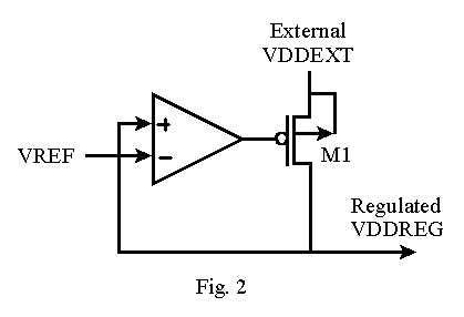
The choice of type P or N for the large driver FET (M1 in Fig. 2) influences the design considerably. The PFET (as shown) is essentially an inverting stage. But as an NFET, it would be a non-inverting source-follower. (Note the polarity of the diff amp inputs is chosen accordingly, so that the path from VREF to VDDREG is non-inverting.)
Because of the stability concerns in CMOS, some have advocated making M1 a large NFET in source-follower configuration. The attraction of this idea is understandable, because it gives significant current gain, and as a source-follower it creates less transport lag in the loop than would the inverting PFET. It also presents less capacitance to the preceding stage, since the Miller effect provides reinforcing coupling from source to gate, rather than the contrarian coupling present in an inverter.
However, for the situations that I am familiar with, I prefer the P type FET for a number of reasons. Due to body effect, the NFET would need a gate voltage higher than the output, and perhaps higher than the external power supply. Oftentimes this would necessitate a boost design as part of the diff amp’s power supply. Also, while the NFET has a smaller transport delay than the PFET, it’s still not negligible.
Finally, we can add a source-follower PFET one stage earlier (M10 in Fig. 6) driving the gate of M1, which accomplishes about the same thing but places the source-follower current gain at a different point in the loop, where its size can be considerably smaller and its biasing levels more consistent with the supply levels.
While it’s important to think about the pole/zero constellation as a theoretical description, a practical evaluation of the circuit requires a Bode plot to show the phase margin.
Recall that when the phase lag reaches 180 degrees, negative feedback turns into positive feedback, making the regulator unstable. As long as the loop gain is less than unity at that point, the oscillations will not increase in magnitude. But we desire that the transient response be not only stable, but also to have good settling behavior. Hence, we’re interested in how far away from that point we are. So, the phase angle difference, from the unity gain point to the 180-degree point, is known as the “phase margin.”
While this was quite simple for circuits in which the gain rolls off monotonically, it is quite possible that in a more complex CMOS circuit the gain curve may reach several local maxima, in which case there may be frequencies for which a unity gain point is much closer to oscillation than we might expect upon first examination. In such a case, very careful evaluation of the Bode plot is necessary.
Figure 4-a is a rough approximation of the root locus for a simple CMOS regulator. There are three zeroes at “infinity,” so the radial distribution sends two of the lines toward the vertical axis as shown. The square boxes mark the approximate location of the roots, for typical CMOS gains. The two located near the vertical axis are the problem, and this topic is consistent with the known low phase margin for the simple CMOS circuit.
A simple capacitor from input to output of a stage forms something like a “transmission zero,” normally a destabilizing effect. However, by adding a resistor of appropriate size in series with the capacitor, we ensure that our zero will appear in the LHP as desired. (This is a somewhat simplified discussion for practical purposes.)
Fig. 5 shows a possible circuit for the reference generator (the second of the three loops in the regulator of Fig. 1.) The addition of R1 and MC10 provides the additional margin that we desire. Practically, it’s best to characterize the phase margin of the overall regulator with a matrix of values of R1 and MC10, and choose the ones that give you the best performance.
Analog design techniques can ensure correct design of CMOS regulation and power control circuits. These basics are increasingly important to those of us who were previously more familiar with digital circuits.
Practical Characterization and Phase Margin

To characterize the phase margin (Fig. 3), we open the loop of the regulator, being careful to keep all existing loads such as the output capacitance, and run a simulation sweeping the frequency at the input, recording the gain and phase delay as seen at the output.
Improving Margin by adding a LHP Zero

We desire to add a zero in the LHP as shown in Fig. 4-b. While the branches tend to get “attracted” toward the zeroes, what’s really happened here is that the total number of zeroes at “infinity” has been reduced from three to two. Thus, the lines depart 180 degrees from each other as shown, and do not move toward the vertical axis.

Now we return to the final stage, with the large output device of Fig. 2, and apply these principles. Fig.6 shows the resulting regulator final stage.

Device M10 is configured in source-follower mode, so it provides some current gain to drive the large gate of M1. IS1 is simply a relaxation path. Devices R4 and MC12 provide a similar phase benefit as discussed previously, and should be characterized over ranges for optimum performance.
Summary
Technical References