Home Products & Services Newsletter About Steve Advance Your Career

Steve Flannagan's
IC Design Journal
Issue #3    November-December 2005

Published by Flannagan IC Technical Services & Consulting, Inc.
WWW.FLANIC.COM
Printable Version:   Issue3 PDF

Dear Friends and Colleagues,
 
Sub-wavelength lithography, ultra thin gates, higher frequencies. Moore’s Law requires us to continue our circuit design techniques for reducing power consumption and leakage. Increased co-ordination is also necessary between circuit design and mask prep as circuit behavior becomes even more geometry dependent.
 
Once again, co-ordination and communication remain the primary attributes for a healthy team environment and a successful business enterprise. Thanks to all of you for your enthusiasm, and for allowing me to be your partner in Technology!
 
Sincerely,
Steve

Business Outlook:

Sub-Wavelength Resolution

For most of the history of photographic science, it’s been common doctrine that the wavelength of light used to create an image must be smaller than the feature being rendered. But in the semiconductor industry, ways have been found to express features much smaller than those for which the equipment was originally intended.

The scaling of feature size has proceeded at a greater slope than the wavelength of light used for photolithography (Fig. 1), crossing over at about 1998. Features are now being printed several times smaller than the wavelength. Techniques have included phase masking, multiple masks, multiple apertures with special shapes, and media with higher refractive indices.

Photolithography trend
Mask Prep and Chip Verification

All indications are that this divergence will continue to widen. Hence, the practice of Mask Prep has become somewhat of a unique specialty itself. As the actual mask data become more removed from your verifiable source, methods for tracking and ensuring a correct design will become more complex, and must be included in your business model.

Breakthroughs in Silicon Technology are often paralleled in other areas. For example, similar resolution improvement has occurred in Scanning Electron Microscopy, where additional information is derived by analyzing the phase and direction of the resultant beam.

Resolution in Other Sciences

Resolution leverage in other basic sciences could be quite interesting. For example, the future of Astronomy may hold new techniques for imaging celestial objects with increased resolution, that go beyond the traditional limitations of the telescopic equations. There are some differences; the spectrum of most astronomical observations is wide, while in mask imaging the wavelength range is quite narrow. And the refractive index of the medium is that of space.

In Particle Physics, a principle limiter was the requirement that a sufficient energy be reached in order to reveal structure below a given level. It would be a benefit if methods could be developed whereby the nature of subatomic particles might be explored with indirect indicators rather than actually reaching that energy.
 
Today's Technical Feature:

Routing and Power Consumption

The continuing progress in smaller features is beneficial for the active transistors, but the effect on metal interconnect has been to increase the resistance to the point that significant delays are experienced in the metal routing.

While “high k” dielectrics are used to improve the gain of active transistors, the field areas now require “low k” dielectrics in order to reduce the capacitance of routing. Also, the shift from aluminum to other metals for interconnect has helped.

The first requirement for good power control is to ensure a judicious usage of metal layers, making an appropriate choice of layers for different purposes. Table I outlines why such metal usage should be consistent throughout a chip design, and indeed over an entire system.

Table I
Metal levels for minimizing power consumption

Level:

Usage:

M1, M2

Strapping, local interconnect

M3, M4

Global signals

M5

Power distribution

M6+

Pads, bussing, chip options


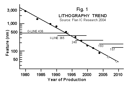
The lowest metal layers are used for source/drain and gate strapping, and for local routing of signals within a circuit block. Higher levels of metal are then used for conveying information over longer distances between blocks, and for power supply routing. Yet another good technique is to use the highest level of metal for bond pads and for options in creating multiple versions of a chip.

As a distribution network expands in a fractal manner, the propagation times to each destination may remain uniform (Fig. 2), but the overall propagation delay and power consumption will be increased.

Thus, it is preferred to distribute the clocks as global signals in high metal, then selectively enable them as local signals in a lower level of metal. Small adjustments in phase (arrival times) can be made in order to align clocks. These techniques may be compared to delay locking.


Fig. 2 Fractal distribution permits equal arrival time
of signals, but causes greater total propagation time
and power consumption. Repeaters may be included.
 
In a digital logic design, phase locking should be used only if no other technique will achieve the desired result. A Delay Locked Loop (DLL) is easier to stabilize because it has only one independent variable (phase.) But it places stricter limits on the frequency range. A Phase Locked Loop (PLL) must converge on two independent variables (frequency and phase) and thus is more difficult to stabilize, but it tolerates a wider range of frequency, which may be useful for power reduction.

You must have a history of experience within your organization before attempting these techniques. That means doing test chips on proposed methods before putting them into an actual product.

Cross Talk

The vertical thickness of metal lines can be greater than their horizontal width. Today’s SEM cross sections show that there is more nearly a parallel plate capacitance to the nearest neighbors than to the ground plane. Appropriate layout techniques are required to assure that the signal is not disturbed.

Co-ordinate Among Chip Sub-Sections

A wide variety of power reduction techniques are presently in use. They include various mixes of selective reduction in supply and frequency. Combinational and Sequential circuits cannot be treated in the same manner. If each section of your chip adopts a different strategy, they could interfere with each other.

You need to ensure that your chip has a consistent power-savings strategy across all sections, and that these methods will not interfere with each other. Also the power-up-clear scheme should be planned in advance, and appropriate conventions adopted for the entire chip.

It is necessary to achieve a consistent global strategy for your clocks. For example, if a sub-circuit receives a masked clock, be sure the mask is cleanly enabled so as not to produce a runt pulse when the clock is in transition. Clocks may also be divided down to lower frequencies where appropriate.

Reduced Signal Swing

The lower power and faster propagation of a reduced signal swing is best realized in scaling the main VDD supply. However, local reduction of the excursion is still beneficial in some circumstances. Fig. 3 calls attention to the power consumed in regulation. Vreg1 is a local regulated level, V1 is a signal name, and Cload is the capacitance of a long metal line. The average current is


  On-Chip Regulation

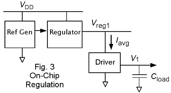
Neglecting the power consumed by the reference generator, the power consumption in the driver and regulator combined is simply
 
Indicating that for local regulated signals, the power reduction is linear with the reduced signal swing, compared with a square law reduction for the case where VDD is scaled. This issue should be considered when deciding whether to regulate Vreg1 off-chip.
 
Reduced Signal Excursion

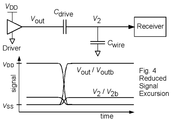
  The Vreg1 regulator can be removed entirely (Fig. 4) but the proportionate reduction in power consumption remains about the same. These circuits would have a mechanism (not shown) to maintain the level of V2. Let the excursion of V2 be VDD / N. Then Cwire / Cdrive will be N-1. The effective driving point capacitance Ceff is then Cwire / N. The power required to operate the circuit is thus
which is 1/N of the power required for a full swing signal. Hence, the scheme of Fig. 4 also scales the power linearly, and not square law, with the signal.

Depending on context and requirements, these signals might be implemented as true/complement pairs, or as single-ended signals with some reference level.

Receiver for Small Signal Swings

A possible receiver design (Fig. 5) accepts the reduced levels on V2 and V2b , then amplifies them with cross-coupled pairs (M2/M3, M4/M5) when the information is needed. We are treating the reduced signals as information content, or data signals, as distinguished from control signals such as the clock CLK/CLKB which are at full rail levels here.
 

Receiver for small signals
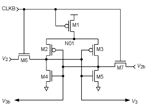
  Fig. 5 Detail of receiver circuit for small signals

This design assumes that the operating level of (V2, V2b) is not above the threshold of M4/M5. (If it were, an additional clocked N-type device could be inserted in the source path of M4/M5 to prevent unnecessary current.) M6/M7 convey the signal level into (V3, V3b) with no threshold drop, because the gates (at CLKB) are at full VDD level, while (V2, V2b) are at reduced levels.

The next stage to receive the amplified signal may have signals that are valid for the full cycle, as would be (V5, V5b) in Fig. 6.
 

Non-RTZ signals
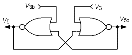
  Fig. 6 Possible latch circuit for next stage
 
Energy Budget in Charge Transfer

Figure 7 compares several types of charge transfer. In each case, Wprovided = Wlost + Wdelivered.

The initial conditions are given as V volts on the left side and 0 volts on the right.

Each sketch must comply with conservation of energy and conservation of charge. From Fig. 7(a) arises the familiar MOS formula of P = CV2f for power consumption, which is independent of the magnitude of R, the resistance of a driver.

In Fig. 7(a) the energy lost and the energy delivered are given as (1/2)CV2 in column 7(a) of table II. While they happen to have the same numerical value, in fact they are not the same energy. One is the energy stored on the capacitance, and the other is the energy expended in the transfer process. Their sum is the energy provided, which is CV2.

In Fig. 7(b) we could also define a term Wretained of (1/8)CV2 and note that Wretained + Wprovided = (1/2)CV2, the energy stored initially on the left capacitance. The total energy stored in the two capacitances after charge sharing is equal to the amount lost in the resistance.

Half-cycle energy budget during charge transfer
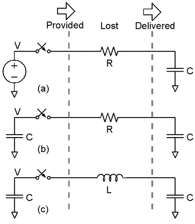
Fig. 7 Energy in charge transfer
 

Table II
Half-Cycle Energy Budget for Charge Transfer


Energy:

7(a)
ordinary

7(b)
sharing

7(c)
reactive

Wprovided

CV2

(3/8)CV2

(1/2)CV2

Wlost

(1/2)CV2

(1/4)CV2

0

Wdelivered

(1/2)CV2

(1/8)CV2

(1/2)CV2


Some "charge sharing" techniques have been described recently in which the two polarities are connected together briefly before switching. The non-idealities would include the power lost in operating the sharing devices, and the need to turn them on and off more quickly than the operation of the driver circuit itself.

Reactive Transfer

Fig. 7(c) illustrates reactive transfer without the associated energy loss. There are many ways in which inductors can be used to reduce power consumption. One such method is shown in Fig. 8, in which the clocks are assisted by the inductor.
 

Resonant clock drivers
Fig. 8 Resonant clock drivers

The resonant frequency might be set to be near that of the clock, or some ratio of it. The period would be given by
Where Ceff = Cload / 2. (For example, T = 2.5 ns, L = 64 nH, and Cload = 5 pF.) In a practical design, CLK and CLKB may have a significant capacitance between them, and so the actual value of Ceff would be computed in a more complicated manner.

MOS drivers would be quite smaller than those normally sized to drive Cload; they would gently keep the clocks energized and synchronized to the input clock. Some power consumption from the drivers would be required in order to make the waveform approximate a rectangular shape; the departures from the sine wave would reflect the extent to which active power is consumed.

Simulations indicate power savings on the order of 10x or better compared with simple driver clocks.

The inductive network could be placed further downstream on the lines to bypass some of the series resistance of CLK and CLKB lines.

Technical References

[1] F.Schellenberg, "A Little Light Magic," IEEE Spectrum, Sept. 2003, pp. 34-39
[2] L. Geppert, "The Amazing Vanishing Transistor Act," IEEE Spectrum, Oct. 2002, pp. 28-33
[3] A. Brown, "Fast Films," IEEE Spectrum, Feb. 2003, pp. 36-40

Career View:

Clever Design Techniques

Creativity is always more beneficial than simple intensity of effort, but we need both in order to keep developing new methods to advance our designs. A world-class business requires similar world-class techniques.

Teamwork is the key behavior for achieving creative designs. The best environment for stimulating thought processes is one in which co-operation is encouraged in design and development teams, as described in my essay, "The Unifying Effects of Teamwork."

You should actively seek out such environments, rather than wait for you superiors or institution to provide them. Review the key questions in our Seminar, “Future-Oriented Career Development,” at www.flanic.com.

This concludes the third edition of Steve Flannagan’s IC Design Journal. We welcome your comments, suggestions, or ideas for future issues. Additional material extending what we have done here will be published in Technical Notes on our web site, or explored further in the next issue of the Journal.

Please contact me for assistance in your technical business, electronic design or team development.

Regards,
Steve


About the writer:

Steve Flannagan is a highly respected electronics designer and consultant, widely acclaimed for his leadership and professionalism. He is especially regarded for his teamwork and dedication to the success of individuals. Steve has designed some of the world’s leading SRAM and memory circuits, is widely published in the field and holds more than 40 United States Patents in the area of circuit design and evaluation. He has worked professionally as a designer at Intel, and also at Motorola where he held the title of Fellow.

Printable Version:   Issue3 PDF

Flannagan IC Technical Services & Consulting, Inc.
POB 200367
Austin, Texas 78720-0367
WWW.FLANIC.COM
Handshake
Professionalism At Its Very Best!  ®

Copyright 2005. The information presented in this newsletter is provided “as is”and “as available.”Flannagan IC Technical Services and Consulting, Inc. makes no representations or warranties of any kind, either express or implied, as to the information, content, presentation, or products included in this newsletter or on this website. Flannagan IC Technical Services and Consulting, Inc. assumes no liability or responsibility for any errors, omissions, or interruptions in the information, content, presentation, or products included in this newsletter or on this website, and specifically disclaims any duty to update the information, content, or presentation, included in this newsletter or on the website. For more information, please see the Terms and Conditions for Use of www.flanic.com.

“Flannagan I.C. Technical Services and Consulting,” “Flannagan IC,” “FlanIC,” “IC Technical,” and the handshake symbol with accompanying words, are trademarks, and “Professionalism at It's Very Best!” is a registered trademark of Flannagan I.C. Technical Services and Consulting, Inc. All other trademarks are trademarks of their associated holders.